Feature
High Aspect Ratio TGV Filling and Inspection Technology
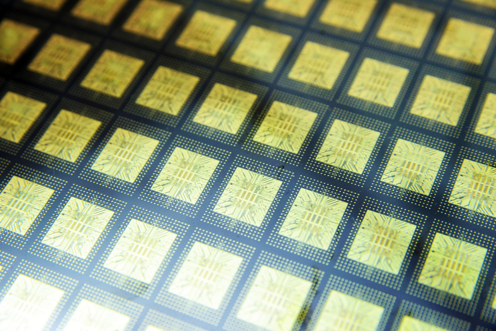
ITRI’s High Aspect Ratio TGV Filling and Inspection Technology increases electrode density and optimizes 3D IC stacking.
In 3D semiconductor packaging, high aspect ratio (HAR) through glass via (TGV) substrate has shown promise as an interposer substrate, providing many advantages over silicon wafer, due to its low dielectric constant, high dimensional stability, ultra-high resistivity, low coefficient of thermal expansion (CTE) mismatch between copper (Cu) material & glass substrate, and good mechanical properties. However, both an all-solution process for HAR TGV with defect-free filling, and a more effective defect inspection method, are still needed.
To address these challenges, ITRI has developed the High Aspect Ratio TGV Filling and Inspection Technology. The TGV filling process uses a simple DC plating waveform with a single plating additive formula to replace the complex PPR (Periodic Pulse Reverse) plating waveform to form the uniformed Cu bridge (butterfly) in the center of TGVs. Moreover, the Cu surface thickness (Cu overburden) can be controlled in the range of 5-10 μm, which is based on the aspect ratio, via size, and substrate thickness. This TGV filling technology employs a full wet process for an aspect ratio (AR) over 15, superior to the commercially available AR between 4-10 that uses both dry and wet processes. ITRI’s full wet process needs only one plating additive formula instead of three types of plating additives (accelerator, suppressor and leveler) required by the conventional formula, reducing the need for complex monitoring of individual formulas and resolving the problem of excessive consumption of plating additives for long-term use.
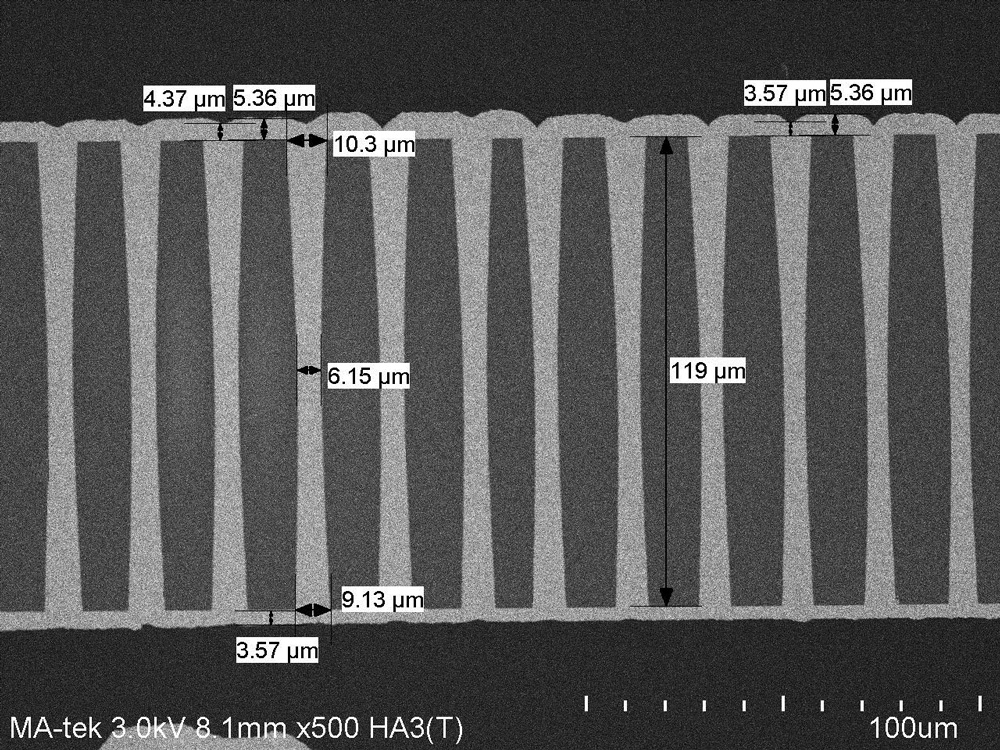
An SEM cross-section image shows that ITRI’s technology has a higher aspect ratio than currently available hole plating processes.
Dr. Meng-Chi Huang, Deputy Division Director of ITRI’s Mechanical and Mechatronics System Research Laboratories, explained that stacking integration of 3D chips is similar to constructing a building, with floors and levels being interconnected by the superstructure and utility lines. The glass substrates are like the “floor panels”, and the through vias in between levels are like the power or water lines that link the entire building. The TGV filling process is therefore an integral part in stacking integration, taking up to 30% of the packaging cost. Dr. Huang stressed that ITRI’s technology has the potential to lower plating cost by 50% compared to current practices.
Apart from TGV filling, defect inspection for the TGV filling process is also crucial. ITRI’s 3D Nano X-ray CT inspection technology performs faster than conventional 3D X-ray interpretation which often takes one to two weeks. Sphere-fitting algorithm is developed to combine with Nano-CT scanning to quickly identify hundreds of defects within one or two hours and achieve a high accuracy. The monitoring system can catch cracks and voids up to 2μm, greatly improving production yield and quality.
ITRI’s High Aspect Ratio TGV Filling and Inspection Technology can be used by those who would like to upgrade advanced semiconductor packaging from silicon wafers to glass substrates, making manufacturers more competitive when entering the global semiconductor packaging, high density PCB and IC substrate supply chains. For its technological breakthroughs and influence on multiple industries, the technology received the Outstanding Research gold medal at ITRI in 2021.