R&D Focus
AI Chip Lab to Accelerate IC Design Process for Industry By Wei-Lun Liang
While a typical IC design follows a standard development process, AI chips need to be designed on a case-by-case basis to accommodate various restrictions for different types of applications. Almost every successful IC design solution for AI products involves automated processing of large amounts of data and information. Yet for smaller companies that intend to provide the full range of IC services from design through manufacturing, it is difficult to develop robust and reliable AI chip designs due to lack of access to advanced tools and verification services.
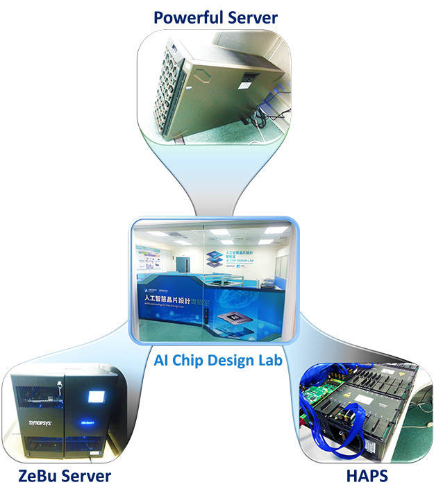
The AI Chip Design Lab operates powerful dedicated servers, ZeBu server, and HAPS prototyping system for design and verification.
To resolve these potential problems when designing high-efficiency AI chips, the AI Chip Design Lab jointly built by ITRI and Synopsys provides necessary assistance, including electronic design automation (EDA) tools such as the hardware accelerated simulation system ZeBu and field-programmable gate array (FPGA) emulation system HAPS for design and verification services, while powerful dedicated servers enable complex computation to handle large scale designs.
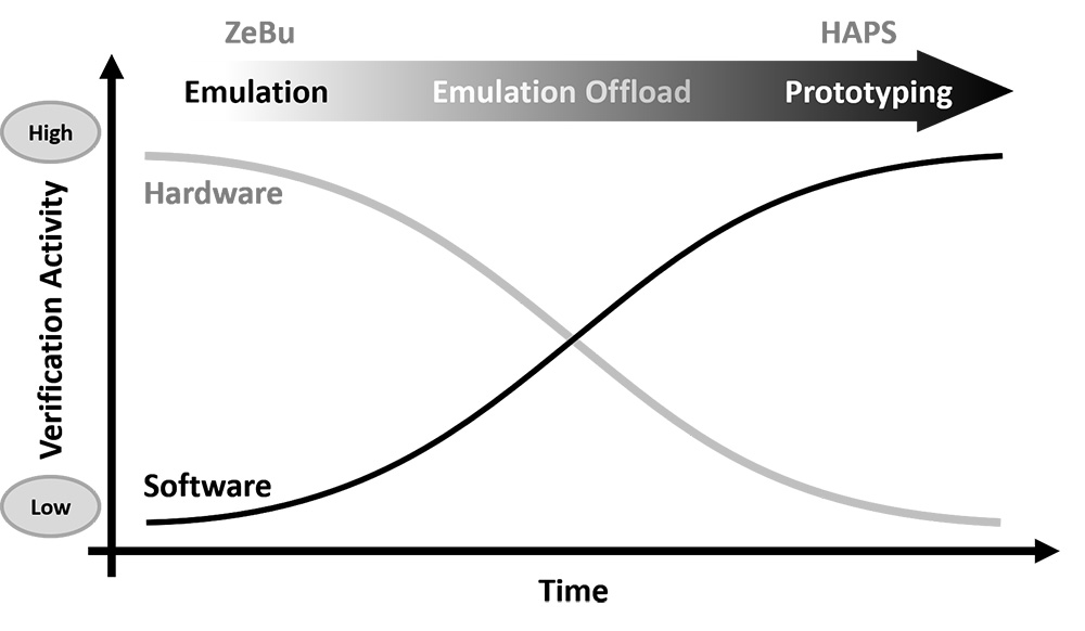
Verification process using emulation and prototyping.
In order to deliver verification services for AI chips, ITRI utilizes Synopsys’ advanced productivity tools (i.e. the ZeBu Server and HAPS system) in the AI Chip Design Lab for FPGA-based emulation and prototyping. As AI chips are specially designed high-performance IC chips made for artificial neural network applications, the verification process for these chips must run through extensive hardware/software emulation and prototyping before production. Engineers use FPGA-based systems for verification when designing an application specific integrated circuit (ASIC), which is an IC chip customized for a particular use such as AI calculations. After the FPGA verification is complete, the design phase is ready for tape-out and a semiconductor fabrication plant can start to manufacture the ASIC chip.
During the ASIC design process, the desired hardware structure is described using the register-transfer level (RTL) code and verified with a hardware emulator system on the ZeBu Server. Once the hardware emulation is completed, software verification is then performed on the HAPS system by applying emulation offload, which transitions the process to prototyping. These emulation and prototyping solutions can help standardize design flows to reduce time to tape-out and speed up design-flow evolution for AI chips.
Combining the strengths of Synopsys’ advanced design tools and silicon intellectual property with ITRI’s design and verification services, the AI Chip Design Lab hopes to assist the semiconductor industry in accelerating the time to market for AI chips and enhancing chip performance. The Lab is poised to improve AI chipset marketing strategies of IC design companies, and will focus on improving the efficiency of manufacturing specialized AI chips for applications including algorithms for robotics, internet of things, and other data-intensive or sensor-driven tasks.
Acknowledgements
I would like to extend my sincere thanks to my manager Ka-Yi Yeh, colleagues Jenn-Shiang Lai, Chia-Yi Yeh and Trung-Hieu Vu. They helped me overcome hurdles, have faith in my abilities, and taught me skills I can further develop in my career. I’d also like to thank Synopsys Principal Investigator Chih-Chung Wei for helping to review this article.
About the Author

Wei-Lun Liang is an engineer working on chip stacking technology at ITRI’s Electronic and Optoelectronic System Research Laboratories. He graduated from National Taiwan University and specializes in electrical engineering and computer science.