Feature
Building Taiwan’s Next Semiconductor Launchpad
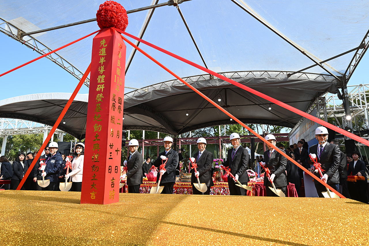
Officials and industry representatives attend the groundbreaking ceremony at ITRI headquarters in Hsinchu, Taiwan.
The Advanced Semiconductor R&D Center has officially broken ground at ITRI’s headquarters campus in Hsinchu, marking a major step toward expanding Taiwan’s semiconductor innovation infrastructure.
Jointly supported by Taiwan’s Ministry of Economic Affairs, the National Development Council, and the National Science and Technology Council, the center is designed to lower verification barriers for small and mid-sized IC design firms and startups, bridging the gap between laboratory research and industrial commercialization.
Beyond IC design houses, the facility will also provide a platform where materials and equipment suppliers can test and validate emerging technologies. By enabling deployment of cutting-edge technologies such as AI chips, silicon photonics, and quantum technologies, the center will further solidify Taiwan’s leadership in the global semiconductor ecosystem.
Scheduled for completion by the end of 2027, the center will deliver three core functions:
- Innovative IC design verification
- Advanced process development
- Localized equipment and materials validation
It will house Taiwan’s first 12-inch advanced pilot line established by a research institution, complemented by upgraded 8-inch facilities. Together, these capabilities will create an integrated environment linking chip design, manufacturing, packaging, and testing.
Speaking at the groundbreaking ceremony, Minister of Economic Affairs Kung Ming-hsin emphasized the Ministry’s role in supporting SMEs and emerging IC design teams by providing access to small-batch, diversified, and application-specific chip prototyping and validation. As a key initiative for these innovators, the new center will offer a one-stop platform integrating chip design, manufacturing, packaging, and testing. It will also allow equipment and materials suppliers to conduct on-site demonstrations and technology validation, accelerating their integration into global supply chains. Through this effort, the Ministry aims to strengthen Taiwan’s semiconductor innovation ecosystem and enhance the resilience and autonomy of its supply chain.
The center will provide 28–90 nm back-end-of-line process R&D and pilot production services, with development cycles expected to shorten by roughly 30%. It will also support a range of frontier technologies—including quantum computing, silicon photonics, ASICs, 3D integration architectures, and next-generation memory.
In parallel, the initiative will deepen collaboration with universities and research institutions, strengthening industry–academia partnerships and expanding the semiconductor talent pipeline.