R&D Focus
World-Record GaN-on-Si Breakthrough for 6G
“When it comes to 6G and direct-to-device satellite communication, it’s all about combining high frequency with long distance to support massive data transmission,” said Shyh-Shyuan Sheu, Division Director at ITRI’s Electronic and Optoelectronic System Research Laboratories.
To achieve reliable high-frequency, long-distance signal transmission, ITRI drew on cross-domain expertise spanning communications, materials, and optoelectronics to develop Ultra-High-Frequency GaN-on-Si Technology. Researchers sought to overcome the power output limitations of conventional semiconductor materials such as silicon and gallium arsenide (GaAs) and enhance the performance of power amplifiers (PAs).
“This is the most challenging research project we’ve ever taken on,” said Dr. Sheu.
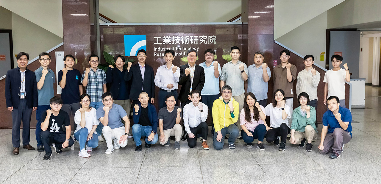
The team behind ITRI’s Ultra-High-Frequency GaN-on-Si Technology and system verification platform
Solving Challenges in Building GaN Transistors
The first challenge was growing the material reliably. Using locally supplied 8-inch silicon substrates, the team grew compound semiconductor layers through quaternary aluminum-indium-gallium-nitride (AlInGaN) epitaxy. Proprietary gas-flow control and a specialized buffer layer improved wafer integrity, increasing the yield from approximately 60% to 100%.
The next challenge was speed. High-frequency switching requires an extremely small gate that also maintains low resistance. The team developed a 39 nm T-shaped gate, compared with the industry mainstream of approximately 120 nm, providing advantages in speed, power consumption, size, and cost.
To support high-speed signal transmission at ultra-high frequencies, an epitaxial regrowth technique was adopted to further reduce resistance at the metal contacts.
A New Milestone for High-Performance PAs and Modules
Once the transistors were completed, the team moved to PA circuit design, using a symmetric power-combining architecture to enhance the stability of the millimeter-wave PAs without compromising the performance of the transistors.
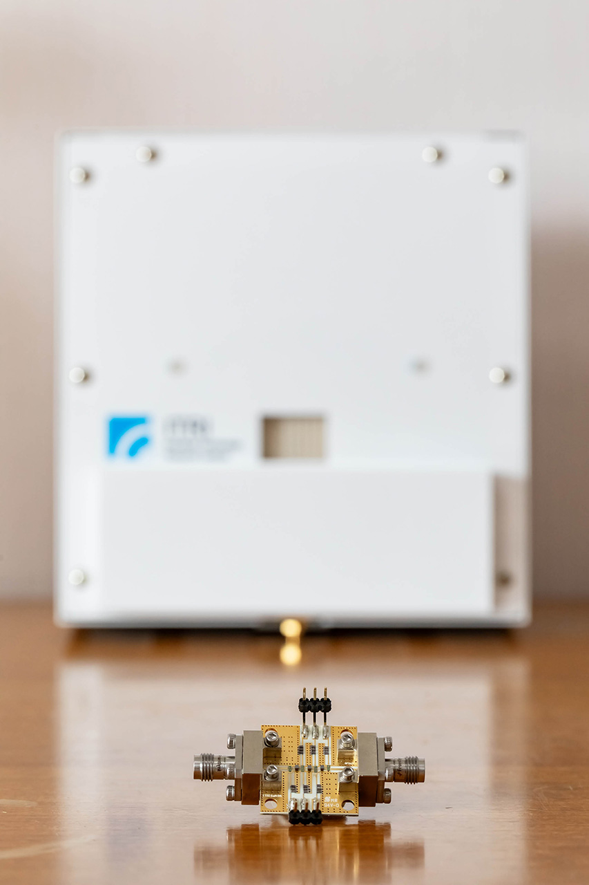
Millimeter-wave PAs made with ITRI’s GaN transistors
Then came packaging. Multiple chips and antennas need to fit into a compact space without allowing heat to become a problem. ITRI’s proprietary antenna-in-package (AiP) technology reduces module size for easier integration into mobile devices. A pioneering thick-copper lead-frame architecture carries heat directly away from the PA.
High-frequency circuits can also create electromagnetic interference. A proprietary EMI suppression material is used to absorb noise rather than reflect it. Combined with a low-loss packaging adhesive, the GaN device extends the frequency capability from 50 GHz to a world-record 325 GHz, with a dielectric loss of only 0.00054, well below the global industry benchmark of 0.0009.
The GaN device can be applied to 100 GHz transmission systems. At the same output power, its millimeter-wave PAs also achieve more than 70% higher efficiency than those of leading international manufacturers.
An Integrated Platform to Accelerate GaN Development
Beyond technical breakthroughs, ITRI has built a GaN integrated device manufacturer (IDM) technology and system verification platform covering epitaxy, device fabrication, circuit design, modules, packaging, materials, and systems.
This end-to-end platform connects Taiwan’s highly specialized semiconductor ecosystem and allows issues at any stage to be quickly identified and addressed, helping companies to shorten development cycles. The platform now enables stable shipments of epitaxial wafers and has supported the spinoff of two startups.
Toward Direct-to-Device Connectivity
The next challenge is to bring the technology closer to personal devices. “We will further shrink the GaN components and reduce their power consumption and voltage,” said Dr. Sheu. “This way, PAs can be embedded into smartphones, smartwatches, and smart glasses to provide direct satellite connectivity for mobile devices.”